
Home > News > Breakthrough in Hermetic Packaging Enhances Image Sensor Reliability
Breakthrough in Hermetic Packaging Enhances Image Sensor Reliability
- In a major leap forward for optical sensing technology, SI Sensors today announced the availability of next-generation hermetic packaging solutions for all their CMOS image sensor developments.
Designed for high-performance imaging in extreme environments, this new generation of truly hermetic vacuum-sealed enclosures provide unmatched CMOS sensor protection against environmental contaminants thereby extending operational lifetime.
“Our hermetic packaging solutions are engineered to preserve the integrity of SI Sensors custom CMOS image sensors in the most demanding conditions,” said Philip Brown, General Manager of SI Sensors. “From space exploration to ultra-high-speed process imaging, these packages enable consistent performance where failure is not an option"
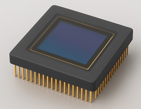
hermetically sealed image sensor package (courtesy: SI Sensors)
Leveraging advanced ceramic-to-metal and sapphire-to-metal sealing techniques, the new packaging designs provide unmatched optical clarity and mechanical strength. Utilization of sapphire windows in the design not only ensures long term operation but also facilitates high transmittance from UV to IR wavelengths. In addition, SI Sensors advanced hermetic packaging solutions incorporate precision die placement with sub-micron accuracy to support advanced optics integration. The new hermetic packaging also provides high thermal conductivity for efficient heat dissipation of ultra high-speed, high-power image sensors.
SI Sensors are a division of Specialised Imaging, focused on innovative CMOS image sensor design and development. The company’s aim is to use its extensive in-house IP and design experience, together with the latest software tools, to design novel image sensors using the most appropriate foundry technologies globally. The full-service CMOS image sensor design offered by the company includes circuit design, pixel optimisation, simulation, layout, verification, and tape-out. In addition, to ensure performance and consistent quality and reliability SI Sensors perform detailed electro-optical testing from characterisation through to mass production testing adhering to industry standards such as EMVA 1288.
For further information please visit www.si-sensors.com or contact the company on +44 1442 827 728 / info@si-sensors.com,
-----------
Worldwide HQ
SI Sensors
Specialised Imaging Ltd.
Innovation Centre
320 Cambridge Science Park
Cambridge CB4 0WG
tel. +44-1442-827728
e: info@si-sensors.com
web: http://www.si-sensors.com
Related News
- Hemodialysis Water Treatment System and Treatment Methods 7/23/2026
- Image Intensifier Helps Advance Fusion Research 7/22/2026
- Titan Enterprises Unveils Next-Generation Hygienic Oval Gear Flowmeters 7/17/2026
- Well-characterised Biospecimens Assist Development of Cancer Immunotherapies 7/10/2026
- Thermo Fisher Scientific Receives First FBI Approval for Rapid DNA Crime Scene P 7/9/2026
- Reproducible Cryopreservation using Alcohol-free Cell Freezing 7/9/2026
- From Cryogenic Synthesis to Photochemistry: Asynt Introduces the New ColdCoil 6/30/2026
- Olympus Launches 4K LCD Monitors to Enhance Clarity in Endoscopic Diagnosis and 6/25/2026
- Specialised Imaging: Ultra-fast High Resolution Video Camera 6/22/2026
- Single Use Support Launches Next-Generation Controlled-Rate Blast Freezer 6/18/2026